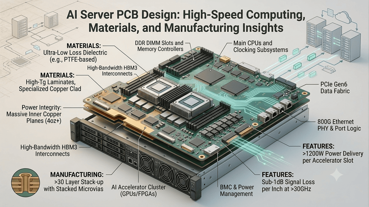
The Critical Role of PCB Reliability in AI Data Centers
The rapid evolution of Artificial Intelligence (AI) training and inference models has fundamentally transformed data center hardware. Modern AI servers powered by advanced GPUs and ASICs process massive datasets at unprecedented speeds. In this high-performance computing (HPC) environment, the Printed Circuit Board (PCB) is no longer just a passive carrier—it is a critical highway for high-speed data transmission and extreme power delivery.
To ensure 24/7 uptime in AI data centers, AI Server PCBs must overcome immense manufacturing challenges:
- Extreme High-Layer Counts: Routing thousands of high-speed interconnects through massive stack-ups without registration failure.
- Signal Integrity (SI): Managing PCIe Gen 5/Gen 6 signaling with ultra-precise backdrilling to prevent data loss.
- Thermal & Power Density: Delivering massive, stable currents (often exceeding 1000W per GPU) while dissipating intense heat.
With over 35 years of precision manufacturing experience in Taiwan, PCE PCB specializes in pushing the physical limits of board fabrication. Capable of manufacturing up to 40 layers and board thicknesses of 6.0mm, we provide the advanced capabilities required to power the next generation of Universal Baseboards (UBB) and AI accelerators.
1. Core Architecture: The PCBs Inside an AI Server
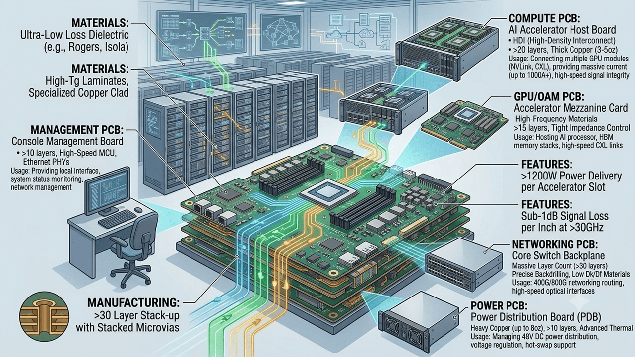
An AI server is a complex ecosystem of specialized electronics. We manufacture tailored PCB solutions for every critical subsystem:
- Universal Baseboard (UBB) / GPU Motherboard: The massive foundation connecting multiple AI accelerators. These demand extreme manufacturing limits (often 24 to 40 layers) and ultra-low loss materials to ensure cross-GPU communication.
- OAM (OCP Accelerator Module) / GPU Boards: Featuring high-density interconnects (HDI), these boards carry the actual AI silicon. They demand perfect microvia registration and aggressive thermal management to prevent throttling.
- Switch Boards & Network Interface Cards (NICs): Responsible for node-to-node communication, requiring precision impedance control to eliminate signal reflection in 400G/800G networks.
2. Mastering High-Speed Signal Integrity & High Aspect Ratios
At PCIe Gen 5/6 networking speeds, microscopic manufacturing variations can ruin signal integrity. Building ultra-thick boards (up to 6.0mm) introduces severe challenges in through-hole plating and signal reflection. We overcome these with industry-leading precision:
- Ultra-Precise Backdrilling:
Unused via stubs act as antennas that reflect high-speed signals. We utilize precision depth-controlled routing with a strict depth tolerance of ±0.05 mm (approx. ±2 mil). This guarantees the removal of reflective stubs without damaging active inner layers.
- 15:1 High Aspect Ratio Plating:
In a 6.0mm thick UBB, ensuring uniform copper deposition deep inside small vias is notoriously difficult. Our advanced plating chemistry and fluid dynamic controls allow us to achieve a highly reliable 15:1 Aspect Ratio, eliminating the risk of barrel cracking or open circuits in high-layer-count boards.
- Tight Impedance Control:
We routinely achieve strict impedance tolerances verified by Time Domain Reflectometry (TDR) testing, combined with low-profile copper foils to mitigate the "skin effect" at high frequencies.
3. Strategic Material Selection: The Isola Advantage
Standard FR-4 cannot survive the high-frequency and high-heat environment of an AI server. As an experienced partner in advanced substrates, PCE PCB leverages the Isola high-performance material portfolio to provide the optimal balance of signal integrity (Ultra-Low Dk/Df) and thermal stability (High-Tg).
| Isola Material |
Performance Category |
Ideal AI Server Application |
|
I-Speed®
|
Low Loss / High-Tg (210°C)
|
Standard AI Server motherboards, PCIe Gen 3/4 interconnects
|
|
I-Tera® MT40
|
Very Low Loss (Df 0.0031)
|
High-speed Switch boards, PCIe Gen 4/5 architectures
|
|
IS580G
|
Ultra Low Loss / Halogen Free
|
OAM Accelerator Modules, High-density 400G network interfaces
|
|
Astra® MT77
|
Extreme Low Loss (Df 0.0017)
|
Next-Gen UBB baseboards, 800G+ Switches, RF/Microwave modules
|
4. Conquering the Heat: POFV and Heavy Copper Technology
AI processors are pushing beyond 1000 watts of Thermal Design Power (TDP). If the PCB cannot effectively move heat away from the silicon, the system will fail. We offer aggressive thermal and power solutions:
- POFV (Plated Over Filled Via) Technology: We expertly utilize POFV (resin plugging capped with plated copper) to place vias directly within BGA pads. This maximizes routing density and creates a direct, highly conductive thermal path away from the GPU into the inner planes, while maintaining a perfectly flat surface for flawless SMT assembly.
- Extreme Heavy Copper (Up to 8oz): To handle the massive power spikes required during intensive AI training workloads, we can manufacture inner and outer layers with up to 8oz heavy copper. This eliminates voltage drops, acts as an embedded heat spreader, and ensures absolute Power Integrity (PI).
5. Extreme Layer Registration & Manufacturing Limits
Pressing a 40-layer, 6.0mm thick board often leads to layer shifting (misregistration) or severe warpage in less equipped facilities. At PCE PCB, our Taiwan facility utilizes advanced CCD inner-layer alignment systems and proprietary press cycles tailored for complex Isola stack-ups. This precise control over dimensional stability ensures perfect pad-to-hole alignment and minimizes board warpage, which is critical when assembling expensive, large-die AI ASICs.
6. Stringent Quality Control & IPC Validation
A single AI server node can cost hundreds of thousands of dollars; a PCB failure is unacceptable. Our QA process ensures zero-defect delivery:
- 100% Automated Optical Inspection (AOI) & TDR Testing.
- Micro-Sectioning Analysis: Rigorously verifying the 15:1 aspect ratio plating thickness and backdrill depth accuracy.
- High-Voltage Isolation Testing: Ensuring robust dielectric integrity between tightly packed, heavy-copper power planes.
7. The PCE PCB Advantage: Taiwan's Trusted Manufacturer
- Geopolitical Supply Chain Security: 100% Taiwan-based manufacturing ensures IP protection and reliable supply chains for global enterprise data centers.
- True HPC Capabilities: Up to 40 layers, 6.0mm thickness, 8oz copper, and POFV mastery.
- Certified Reliability: ISO 9001 and UL certified, manufacturing to stringent IPC-6012 Class 2 and Class 3 high-reliability standards.
Accelerate Your AI Hardware Development with a Proven Partner
Don't let manufacturing limitations dictate your AI server design. As a highly experienced manufacturer with extensive, proven expertise in AI Server PCBs, PCE PCB is committed to delivering uncompromised quality and strictly controllable lead times. We ensure your critical HPC projects stay on schedule without ever sacrificing reliability.
Partner with us to push the boundaries of layer counts, high-speed materials, and extreme power delivery.
Contact PCE for engineering support and quotations today.
|