PCE uses Polar Impedance Calculator SI8000 to simulate the most appropriate parameters base on clients’ needs. With more than 20 years of manufacturing Impedance control PCB, PCE collects lots of DATA which affect the performance of Impedance such as prepreg’s thickness change before and after the lamination.
PCE provides free Impedance calculation for all clients before making sample (pilot run). We also use the sample outcome to improve the accuracy for mass production.
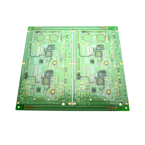
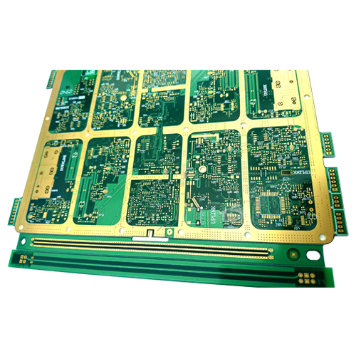
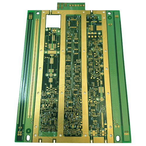
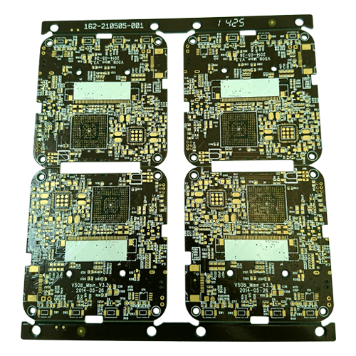
Rigid PCB Capability
| Feature |
Capability |
| Lamination |
Layer count |
1-32 layers |
| Min. thickness |
4 mil(0.1 mm) |
| Max working panel size |
24x31.5 inch(610x800mm) |
| Max. aspect ratio |
10:1 |
| Copper |
Copper Thickness |
0.33~3.0 oz (11~105um) |
| Trace |
Min. Line Width /Space |
3/3 mil |
| Routing |
Dimension tolerance |
+/- 2 mil (0.05mm) |
| Solder Mask |
S/M minimum dam width |
2.5 mil |
| Impedance Control |
Differential pair |
+/- 10% |
| Mechanical Drilling |
Min. drilling hole size |
4 mil(0.1mm) |
| 3 Axis |
Depth control accuracy |
+/- 2mil (0.05mm) |
| Material Availability |
FR-4, High Tg FR-4, Halogen-free FR-4, Metal Core, Low Dk/Df (ISOLA/ Rogers) |
| Finish Availability |
Lead-free HASL, HASL, OSP, ENIG, Pattern Gold Plating, Immersion Silver/Tin, Carbon Ink |

inquiry